The Layman's Guide to IC Reverse
Engineering has been created to teach you the very basics of what it
takes to reverse engineer integrated circuits. Not too much particular focus is
given to the physics and math, just the bare essentials for a layman to turn
images into logic. And chips into images. Kudos to academia, security
researchers, and chip enthusiasts from around the world for all their papers and
presentations that this effort draws inspiration from.
Please reach out with corrections and comments to adc@intruded.net
The Idea
An interesting property of ICs is that their functionality
can be deduced from imaging their structure. This can be done with optical
microscopes for ICs with big fat transistors. These ICs tend to be either simple
or old. Whereas a Pentium I had a process size of 1um (easily viewable), today
intel is rolling out a process size of
22nm in Ivy Bridge. That is just a factor of 10 away from the width of DNA (the
topic of the next Layman's guide, of course).
Once these images are extracted, the relevant portions can be manually turned
back into the abstract. Or, if the target is complicated, the images can be
simulated using custom tools and existing software.
The hardest part about this is having some practical experience to quickly
recognize various structures in images. This can require intense concentration
and insight for the unenlightened. But once you see the patterns, then it's easy
mode. That is where this guide comes in.
Tools for learning
layout
Tools are great. You'll need to grab some to get
started with this tutorial. For now, this section focuses on magic, a layout
tool; and irsim, a simulator that works with magic.
Since hooking up a
logic probe to the insides of a microchip can be a bit nuanced, simulators are
often a better route. The downside is that the layout must first be captured. But
we're getting ahead of ourselves already.
Both of these tools are available from opencircuitdesign.com. There, you'll also find
other maintaned repos of unix software for digital design.
Feel free to
send in your suggestions or writeups on other free tools, such as klayout or
degate.
Magic
"Magic, the VLSI layout editor,
extraction, and DRC tool. "
Magic is a lambda-based layout editor.
It is designed to work for an arbitrary process size on a variety of technology types.
From what I understand, the lambda unit approach breaks down for designing
nanometer technology, but that's okay.
One particulary nice thing about
magic is that it allows laziness. Details about wells and other things can be
omitted, and magic will figure it out. Follow the instructions to build it.
Building
 git clone git://opencircuitdesign.com/magic-8.0

 cd magic*; ./configure --with-x --x-includes=/usr/X11/include/X11/
--x-libraries=/usr/X11/lib/
 make
make install
Note, when I
built magic on Mac OS 10.6, I ran into 64-bit issues at runtime due to a missing header or
something and had to modify the configure script (which resets CFLAGS) to build
in 32-bit mode.
Be sure to seek out the tutorials magic comes with and breeze
through them to understand boxes, cells, etc.
IRSim
"IRSIM, the
switch-level digital circuit simulator. "
IRSim is key for what we're about to do. Since we're just learning IC design,
it's nice to have a tool that can simulate our layouts so we can verify our
assumptions.
Building
    git clone git://opencircuitdesign.com/irsim-9.7

    cd irsim*; ./configure --x-libraries=/usr/X11/lib/
--x-includes=/usr/include/X11/ --without-tcl
 make
 make install
Note that I don't use tcl. You might want to give it a shot,
but i've been leaving it out as a non essential. A fun fact is that magic, Tcl,
and Tk were all written by the famous John Ousterhout.
CMOS Layout
By far the most common technology today is CMOS, so let's get
going on understanding how it looks.
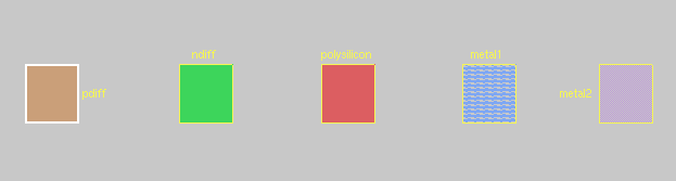
Materials
(materials as seen in magic)
Charge carriers:
Electrons are particle-waves of
energy which we label negatively charged. When current is flowing, that means
electrons are being transfered through a medium.
Electron Holes are the absense of
electrons. They actually have more effective
mass than electrons do (the wave vector math and physics is a bit beyond me).
Just as you can imagine electrons flowing through a medium, you can think of the
dual -- electron holes flowing.
Silicon
N-type -- Negatively
doped silicon produces an abudance of negative charge carriers
P-type --
Positively doped silicon produces an abundance of positive charge carriers.
Metal - metals are good conductors. Wires are built from metal to route
signals across a circuit. Contacts are also made out of metal as well as vias --
which are vertical structures that connect the layers underneath. Transistor
gates are sometimes made out of various metals as well.
Polysilicon is
used to form the gates of transistors.
Notes for reversers
Electron holes have more effective mass, and
therefore less mobility. P-type regions are thus made bigger than N-type regions
to compensate. The size disparity often differentiates P-type and N-type silicon.
Putting it all together
This is a contrived example of a
p-channel mos transistor (PMOS). The brown is the p-type diffusion (pdiff). The blue
is metal1. The red is the polysilicon (labeled gate). And the black x with the
box labeled "contact" connects the metal to the pdiff layer.
When the
red strip has a high voltage applied, current does not flow through the metal
contact to the other side of the strip. When the red strip has a low voltage
applied, current does flow to the other side.
As shown above, we could use this to get output where labeled in the diagram. In
effect, if the gate had a low voltage applied, we would get a high value at the
output. Otherwise, the output would be in a high impedance state.
The gate acts as a valve. On either side of the gate is p-type silicon. Underneath the gate is not p-type silicon, but n-type silicon. When a low voltage is
applied to the gate, a channel of electron holes will be formed bridging the two sides of the gate. When a high voltage is applied, the valve is turned off, and
this channel disappears, isolating the sides from one another. Cool!
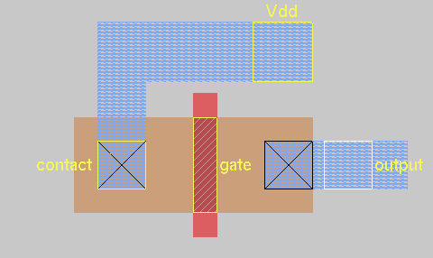
Alright, now that things are getting interesting, let's take a look at an n channel mos
transistor (NMOS).
You can think of nmos as
the dual of pmos. When the red polysilicon strip has a high voltage applied to it, current
will flow through to the other side. When the red strip has a low voltage
applied to it, current will not flow through. This is the opposite gate
relationship from what we saw before.
Note that now, the metal at the
top has a low voltage applied (Gnd/ground) versus a high voltage (Vdd/power). So, if the gate has a
high voltage applied, the output will be low. Otherwise, the output will be in a
high impedance state.
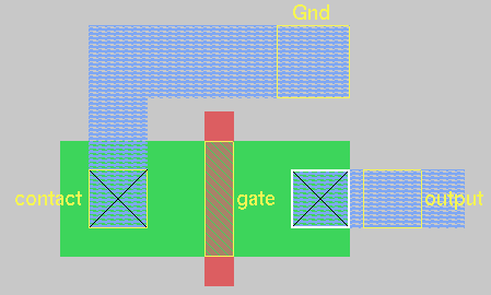
There are also some other properties which
make associating NMOS with Gnd contacts (rather than VDD) more desirable, but we
don't need to worry about that too much. Unless you're looking at some really
strange CMOS, you can always expect to see NMOS tied with ground rails and PMOS
tied with power raOAils.
Complimentary, the C in CMOS,
refers to using PMOS and NMOS transistors in pairs for extremely power efficient
logic gates. Let's take a look at how that works with an inverter
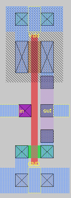
Inverter Layout
An inverter provides the negated input at its output. In the realm of digital logic,
this means high output for low input, and low output for high input. These values vary
upon the technology but you can think of 0V as low and 5V as high if you need a reference.
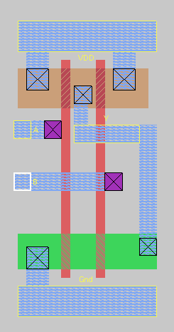
By combining together the two pieces shown above, we can build a CMOS inverter.
Many guides are around for building an inverter with Magic. I found this one
particularly helpful.
In the end, you should end up with this: For your convenience, I've uploaded the magic file
here: inverter.mag
Inverter Simulation
Open up the
inverter in magic, and then run the following commands
:extract all
:ext2sim inverter.ext
%irsim scmos100.prm inverter.sim
Great, now you're ready to simulate. Repeat by copying the commands below.
  *** IRSIM 9.7.73 *** @ Thu Apr 28 20:44:35 PDT 2011 Warning:
Aliasing nodes 'GND' and 'Gnd' inverter.sim: Ignoring lumped-resistance ('R'
construct)

Read inverter.sim
lambda:1.00u format:MIT 4 nodes; transistors: n-channel=1
p-channel=1 parallel txtors:none
irsim> s
time = 10.000ns
irsim> w in out
irsim> s
out=X in=X
time = 20.000ns
irsim> w gnd vdd
irsim> s
Vdd=1 Gnd=0 out=X in=X
time = 30.000ns
irsim> l in
irsim> s
Vdd=1 Gnd=0 out=1 in=0
time = 40.000ns
irsim> h in
irsim> s
Vdd=1 Gnd=0 out=0 in=1
time = 50.000ns
If you'd like a visual of your signals, you may also appreciate the analyzer
command
irsim> analyzer in out
This should convince you that your layout worked, at least enough for irsim
to understand what you meant. With this powerful tool you can now observe and set
nodes to various voltage levels.
The commands to do this are h,
l, x, and u for high, low, high impedance, and unknown. For
a rundown on commands, just type help from within rsim (and help command for more
information on a particular command).
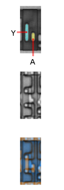
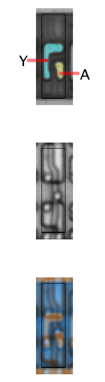
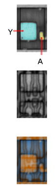
Real world inverters
Let's take a peek at some of the real world examples from the silicon zoo. Reproduced here, (currently
without permission)
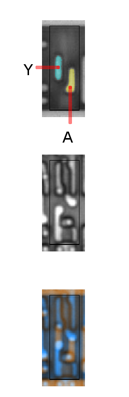
For each of these
images, three views are shown. The top view is the metal layer. The middle view
is with the metal removed, exposing the silicon. The bottom view is a mash up of
the top two.
Start from the left image, and try to figure out how each
resembles the inverter sketched in Magic above. Work your way towards the right
image.
If you're having trouble seeing it, first focus on finding the
gate (red strip in the magic screenshots). Next, determine which one is the
P-type silicon and which one is the N-type silicon. Last, realize that the
contextual information about power/ground is missing here and you have to make a
guess. Now you should be able to figure out the input/output transfer function.
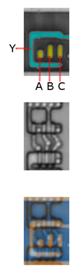
If you still need a hint: A is the input, Y is the output.
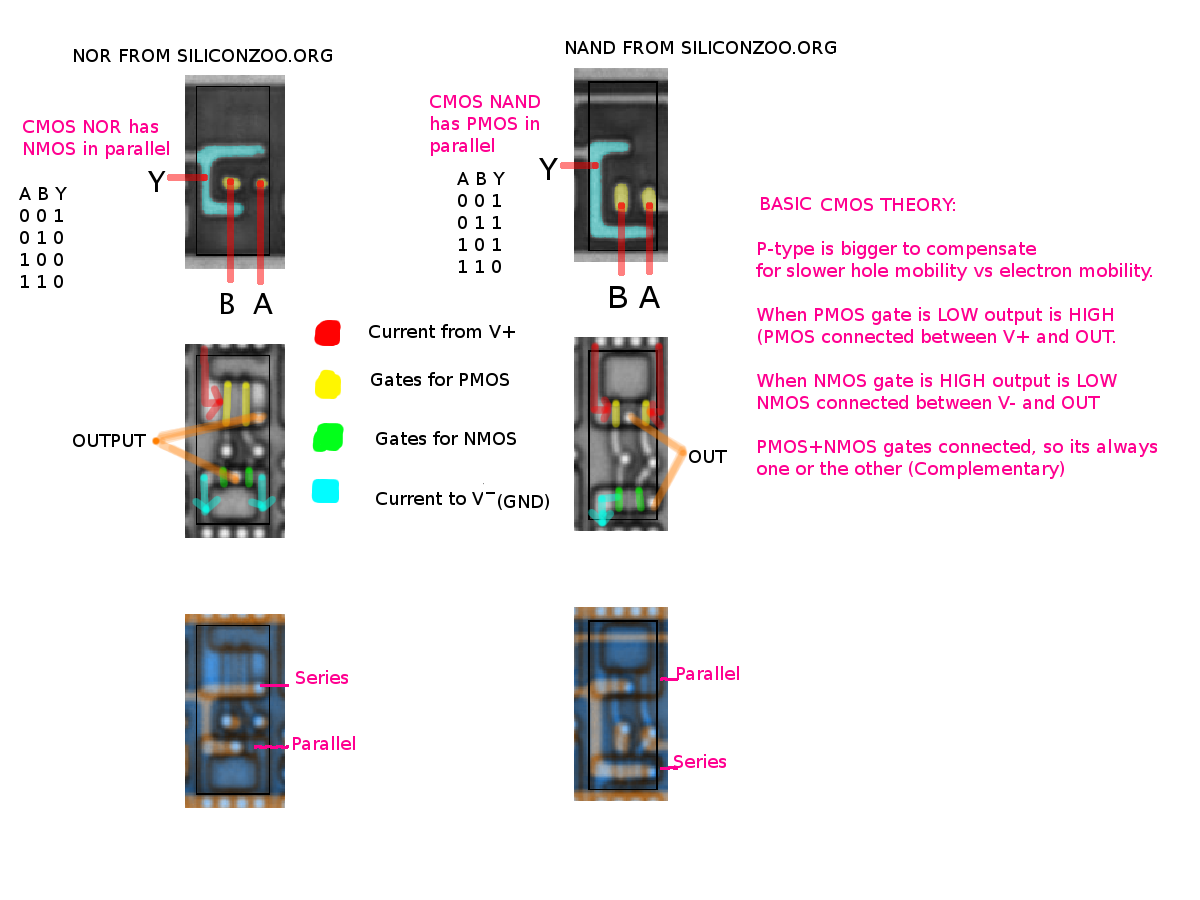
Alright, I admit it, the rightmost picture doesn't make any sense. But the other
three should be very clear! In the real world, it seems things aren't so square.
These shapes are quite messy.
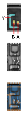
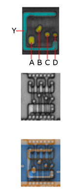
Alright, you know the drill. Start from the left,
and work your way to the last image. For each one, identify the gates. Next,
identify the pmos vs nmos. And last, trace the path current would take during a
state transition.
If you find that you're struggling, open up magic and give
it a whirl. Reconstruct the structures that you see. Then run the simulator.
If you'd like to cheat, here's an image to walk you
through NOR vs NAND.
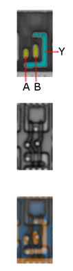
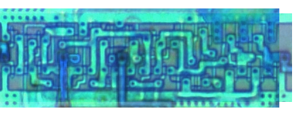
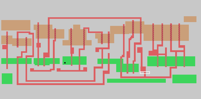
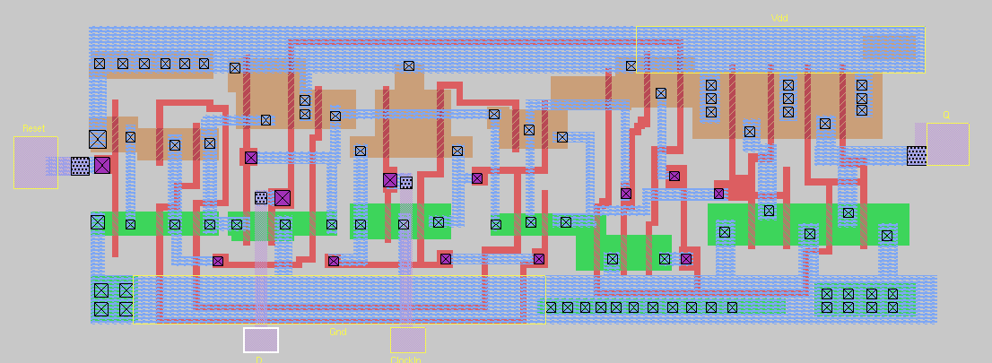
The FlyLogic
Challenge
Alright ladies and gentlemen, now we're going to take
a complex image and see if we can deduce its functionality by using magic+irsim.
The target again comes from the zoo folks, and was a challenge given on the flylogic blog
What you're viewing is a D flip
flop (as previously solved on the flylogic blog by the winner, Jeri).
On the far right is the output, labeled Q. On the bottom middle, we have D (the
input) and ClockIn (clock). The leftmost input is a Reset line. It is used to put
the flip flop into a known state. When low, it resets the output Q to 0.
All that is left is running the simulator to verify our results. Lets get
going
Run magic on the download, and enter these commands to make the
sim file and run the simulator
 w D ClockIn Reset Q ana D ClockIn Reset Q clock
ClockIn 0 1 c
Great, the output shouldresemble this
irsim> c Reset=X ClockIn=1 Q=X D=X
Now you're ready to use the flip flop.
irsim> h Reset
irsim> c Reset=1
ClockIn=1 Q=X D=X
time = 40.000ns
irsim> l D
irsim> c
Reset=1 ClockIn=1 Q=0 D=0
time = 60.000ns
irsim> h D
irsim> c
Reset=1 ClockIn=1 Q=1 D=1
time = 80.000ns;
there are 1 pending events
irsim> l D
irsim> c
Reset=1 ClockIn=1 Q=0 D=0
time = 100.000ns
irsim>
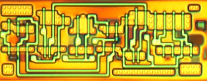
So, how to distinguish inputs and outputs? Well, inputs tend to be tied to
gates (not always, but often). Outputs, on the other hand, will not be, and will
be buffered well. Take a look at the right side, you can see the node labeled Q
in between power wires on the pmos and in between ground wires on the nmos.
Definitely an output. As for the other three, they are each directly controlling
gates.
If you have questions about any part of this process, please let
me know.
What's Next
So far this tutorial has provided you with the mental and software tools to simulate CMOS transistors, with references to work from.
This skill is just one of many a silicon reverse engineer must employ to analyze a circuit. Silicon dies must also be extracted from packages.
High quality image captures of the different layers must be made. And on the imaging side, redundancy should be automated where possible
to accelerate the process.
Decapping
Disclaimer
Please read the siliconpr0n Disclaimer :
Many of the procedures on this Wiki are extremely dangerous and should not be attempted except by trained professionals. We take no responsibility for accuracy of the information including, but not limited to, any safety precautions or other procedural notes that may result in personal or material damage. Do not attempt these procedures unless you are certain that you can do so safely without damage to yourself, others, and/or your surroundings.
Decapsulation refers to extracting the silicon die from its package. If the chip you're looking for is in a plastic card, a pint of acetone will do the trick.
If the target is encased in an epoxy carrier, it won't be that simple. The wiki will help you there with a number of known techniques. Normally, these methods
only need to be used when tools are otherwise unavailable. Research facilities and testing firms have equipment which will take care of this for you.
Once a silicon die is extracted, each layer needs to be captured. For microprocessors, there can be a dozen different metal routing layers, this can be quite
daunting. Each layer needs to be captured to figure out how nodes propagate across the circuit layout. Protective layers must also be removed. The wiki has
more informationa bout this.
Excellent image captures make analysis easy! Poor images do not lend
well to reverse engineering, and can not be automatically extracted
from.
A typical set up involves a digital camera hooked up to a
microscope with a sample that is attached to programmable controls.
Software automates grabbing the full image as a set of tiles across a
rectangular grid by moving the scope or sample and engaging the camera.
Stitching must then be applied to all these tile images to form
one very large image. This makes later analysis easier. Various
stitching tools, such as hugin, are essential for this
process.
A successful stitch marks one image capture. If there are occluded
layers, this process must be repeated for each layer underneath. For
example, one capture may get the top metal layer. Then, this layer must
be removed (by machining, or other means). And then, then another iamge
is made of
the die with the newly exposed layers. Staining can also be applied to bring out materials and features that are otherwise difficult to identify.
These images are then ready to use with tools such as degate, which helps automate logic cell detection and routing.
If the goal is to simulate the system at the transistor layer, the full IC layout can be extracted using Photoshop, GIMP, or a layout editor such as magic.
Magic is quite powerful, and you should consult the tutorials. If you're feeling really lazy, to get started,
you need a mouse (preferably with 3 buttons). Press "space" to switch between tools. By default you'll be using the
box tool, it looks like a cross. Left click picks the lower left corner of the box. Right click picks the upper right corner
of the box. In this mannery arbitrary boxes can be drawn on the layout.
To paint something inside the box, use the :paint command. Just type :paint _layer_, where _layer_ is based on the current
technology file. For cmos, try ndiff, pdiff, polysilicon, polycontact, metal1, or metal2. A middle click will copy whatever material you clicked
on into the current box. Hit "space" to the routing tool. Middle clicking on a different layer will automatically create the correct via or contact
for the current box with the layer you clicked on.
You can zoom in and out with the :zoom command, or the z/v keys. You can use the "s" key to select different structures
and "c" to copy them around. Note that the key combinations vary across magic distributions
and many configuration settings (YMMV greatly).
Last, you can label things with the :label command. But seriously, read the tutorials, there is a wealth of information there, such
as cells, routing, advanced copy commands, and integrated use of irsim.
Lambda what?
Lambda is a unit-less quantity representing the smallest possible dimension in a circuit.
How does this MOS transistor actually work?
Wikipedia has a great discourse on the MOSFET. If you're confused
by the cross sections, remember that you're seeing this all from a top down view. This guide does not mention the wells/substrate
layers underneath that are critical for the whole operation.
 (materials as seen in magic)
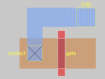